 sales@aoelectronics.com
 +86 755 2821 9272


Manufacturers
- Abracon
- Adam Tech
- Aerospace, Defense & Marine
- Agastat
- AIC
- AKM Semiconductor
- Alcoswitch
- Allegro
- Alps Electric
- Altera
- AMI Semiconductor
- AMP
- ams
- Analog Devices (ADI)
- Aptina Imaging
- Atmel
- Avago / Broadcom
- AVX
- Axicom
- Bccomponents
- Beyschlag
- BI Technologies
- Bourns Inc.
- Bowei Integrated Circuits
- Bridgelux
- Buchanan
- California Micro Devices
- Catalyst Semiconductor
- CGS
- Cirrus Logic
- Citizen Electronics
- CML Microcircuits
- Coiltronics
- Cooper Bussmann
- Corcom
- Core Logic
- Cree
- CSR PLC
- CTS
- Cypress Semiconductor
- Dale
- Data Image
- Deutsch
- Diodes Incorporated
- DOMINANT Opto Technologies
- E-T-A
- Eaton
- ECS
- Edison Opto
- Elcon
- EPCOS
- Epistar
- Epson
- Everlight Electronics
- Exar
- Fairchild Semiconductor
- FCI
- Freescale Semiconductor
- Fremont Micro Devices (FMD)
- Fujitsu Semiconductor
- Fulltech Electric
- General Semiconductor
- Harvatek
- Holsworthy
- Hsuan Mao Technology
- IDT
- Infineon Technologies
- Innolux
- International Rectifier (IR)
- Intersil
- IRC
- ISSI
- IXYS-IC
- Jing Cheng Electronical
- JL World
- Johanson Dielectrics
- Johanson Technology
- JRC / NJR
- JST
- KEC
- Kilovac
- Kingbright
- Kyocera Industrial Ceramics
- LEDiL
- Linear Technology / ADI
- Lite-On Technology
- Littelfuse
- Lumex
- Lumileds
- Luminary Micro
- Luminus Devices
- Macronix
- Maojwei / ZJPT
- Maxim Integrated
- MCC
- Mean Well Enterprises
- Microchip Technology
- Micron
- Microsemi
- Mini-Circuits
- Molex
- Murata Manufacturing
- Murata Power Solutions
- MWT
- National Semiconductor
- Nichicon
- Nippon Chemi-Con
- NJR / JRC
- NVE
- NXP Semiconductors
- OEG
- Omnivision
- ON Semiconductor
- Optek Technology
- Optrex
- OSRAM Opto Semiconductors
- OTAX
- Panasonic
- Peregrine(pSemi)
- Potter & Brumfield
- Power Integrations
- PowerStor
- Preci-Dip
- Prewell
- Products Unlimited
- Pulse Electronics
- PulseCore Semiconductor
- Qorvo
- Raychem
- Renesas Electronics
- RFMD
- Richtek Technology
- ROHM Semiconductor
- Rubycon
- Samsung Electro-Mechanics
- Samsung Semiconductor
- Schaffner
- Schrack
- Seiko Instruments, Inc. (SII)
- Semtech
- Sensata
- Seoul Semiconductor
- Sfernice
- Sharp Display
- Sharp Microelectronics
- Silicon Labs
- Siliconix
- Skyworks Solutions
- SoniCrest / JL World
- Spansion
- Sprague
- Stanley Electric
- STMicroelectronics
- Sunny Electronics
- Susumu (SSM)
- Taimag
- Taiyo Yuden
- TDK
- TDK-Lambda
- TE Connectivity
- Teccor
- Texas Instruments (TI)
- Thin Film
- Tianma Micro-electronics
- TOCOS
- TOKO
- Toshiba Electronic Components
- TT Electronics
- Tusonix
- TXC
- Tyntek
- Vishay
- Vishay Precision Group
- Vitramon
- Walsin Technology
- Weidmuller
- Welwyn
- Wickmann
- Winbond
- Xilinx
- Yageo
- Zetex Semiconductors
- ZJPT / Maojwei
News
Toshiba‘s Electrostatic Discharge (ESD) Protection Device with 0.13μm Process for Analog Power Semiconductor Improves ESD Characteristics
2016-06-15 | ReturnInjections of ESD surges, whether from the human body or equipment, have the potential to destroy semiconductor devices, as ESD current flows cause local temperature increases inside silicon. ESD protection devices are required to protect internal circuit. This is especially true for analog power semiconductor devices required to apply 10V to 100V, which need a high rated voltage. In this case, ESD protection devices must ensure high current flow, which results in enlarged chip size. Shrinking the size of the ESD protection device is an issue in realizing more compact chips.
Using 3D simulation analysis of an ESD event, Toshiba found out that ESD induced destruction is caused by lattice temperature increase due to the current flowing at the highest electric field point. Modifying the transistor structure, which extending the drain low resistive region to the source direction and suppressing the lateral silicon resistance, shifts the current flow from the bottom of the drain to source direction and detaches it from the highest electrical field point. This optimized design was found to increase ESD robustness by up to four times and to decrease the standard deviation down to 1/12. In addition, the device size required to ensure HBM* ±2000V was cut by 68%.
Toshiba offers advanced analog process platforms, with 0.13μm process technology, that can be embedded with the transistors such as CMOS, DMOS, bipolar transistor and the passive devices such as resistor and capacitor. User can select a process suited to each application from three process platforms: “BiCD-0.13” is mainly for automotive (DMOS line up is up to 100V); “CD-0.13BL” is mainly for motor control drivers (DMOS line up is up to 60V); and “CD-0.13” process is mainly for power management IC (DMOS line up is up to 40V).
Toshiba plans to release products using the CD-0.13 process applied in this technology in 2017 and proactively continue to implement to other process platforms to improve electrostatic discharge characteristics.
* HBM (Human Body Model) : one of the parameter to indicate ESD robustness
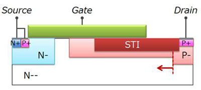
Fig.1 Schematic cross-section of studied structure.
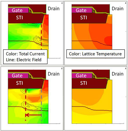
Fig.2 3D-Simulation results for studied structure.
Source:http://www.semicon.toshiba.co.jp/eng/