 sales@aoelectronics.com
 +86 755 2821 9272


Manufacturers
- Abracon
- Adam Tech
- Aerospace, Defense & Marine
- Agastat
- AIC
- AKM Semiconductor
- Alcoswitch
- Allegro
- Alps Electric
- Altera
- AMI Semiconductor
- AMP
- ams
- Analog Devices (ADI)
- Aptina Imaging
- Atmel
- Avago / Broadcom
- AVX
- Axicom
- Bccomponents
- Beyschlag
- BI Technologies
- Bourns Inc.
- Bowei Integrated Circuits
- Bridgelux
- Buchanan
- California Micro Devices
- Catalyst Semiconductor
- CGS
- Cirrus Logic
- Citizen Electronics
- CML Microcircuits
- Coiltronics
- Cooper Bussmann
- Corcom
- Core Logic
- Cree
- CSR PLC
- CTS
- Cypress Semiconductor
- Dale
- Data Image
- Deutsch
- Diodes Incorporated
- DOMINANT Opto Technologies
- E-T-A
- Eaton
- ECS
- Edison Opto
- Elcon
- EPCOS
- Epistar
- Epson
- Everlight Electronics
- Exar
- Fairchild Semiconductor
- FCI
- Freescale Semiconductor
- Fremont Micro Devices (FMD)
- Fujitsu Semiconductor
- Fulltech Electric
- General Semiconductor
- Harvatek
- Holsworthy
- Hsuan Mao Technology
- IDT
- Infineon Technologies
- Innolux
- International Rectifier (IR)
- Intersil
- IRC
- ISSI
- IXYS-IC
- Jing Cheng Electronical
- JL World
- Johanson Dielectrics
- Johanson Technology
- JRC / NJR
- JST
- KEC
- Kilovac
- Kingbright
- Kyocera Industrial Ceramics
- LEDiL
- Linear Technology / ADI
- Lite-On Technology
- Littelfuse
- Lumex
- Lumileds
- Luminary Micro
- Luminus Devices
- Macronix
- Maojwei / ZJPT
- Maxim Integrated
- MCC
- Mean Well Enterprises
- Microchip Technology
- Micron
- Microsemi
- Mini-Circuits
- Molex
- Murata Manufacturing
- Murata Power Solutions
- MWT
- National Semiconductor
- Nichicon
- Nippon Chemi-Con
- NJR / JRC
- NVE
- NXP Semiconductors
- OEG
- Omnivision
- ON Semiconductor
- Optek Technology
- Optrex
- OSRAM Opto Semiconductors
- OTAX
- Panasonic
- Peregrine(pSemi)
- Potter & Brumfield
- Power Integrations
- PowerStor
- Preci-Dip
- Prewell
- Products Unlimited
- Pulse Electronics
- PulseCore Semiconductor
- Qorvo
- Raychem
- Renesas Electronics
- RFMD
- Richtek Technology
- ROHM Semiconductor
- Rubycon
- Samsung Electro-Mechanics
- Samsung Semiconductor
- Schaffner
- Schrack
- Seiko Instruments, Inc. (SII)
- Semtech
- Sensata
- Seoul Semiconductor
- Sfernice
- Sharp Display
- Sharp Microelectronics
- Silicon Labs
- Siliconix
- Skyworks Solutions
- SoniCrest / JL World
- Spansion
- Sprague
- Stanley Electric
- STMicroelectronics
- Sunny Electronics
- Susumu (SSM)
- Taimag
- Taiyo Yuden
- TDK
- TDK-Lambda
- TE Connectivity
- Teccor
- Texas Instruments (TI)
- Thin Film
- Tianma Micro-electronics
- TOCOS
- TOKO
- Toshiba Electronic Components
- TT Electronics
- Tusonix
- TXC
- Tyntek
- Vishay
- Vishay Precision Group
- Vitramon
- Walsin Technology
- Weidmuller
- Welwyn
- Wickmann
- Winbond
- Xilinx
- Yageo
- Zetex Semiconductors
- ZJPT / Maojwei
News
Expansion of the lineup of 80 V N-channel power MOSFETs with the adoption of a new process that helps to improve the efficiency of power supplies : TK2R4E08QM, TK3R3E08QM, TK5R3E08QM, TK7R0E08QM, TK2R
2021-03-31 | Return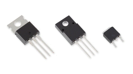 switching power supplies of industrial equipment. Three package types are available: “TK2R4E08QM, TK3R3E08QM, TK5R3E08QM and TK7R0E08QM” using TO-220, a through-hole type; “TK2R4A08QM, TK3R2A08QM, TK5R1A08QM and TK6R8A08QM” using TO-220SIS, an isolated through-hole type; and “TK5R1P08QM and TK6R9P08QM” using DPAK, a surface mount type.
By adopting the new generation U-MOSⅩ-H process with a low-voltage trench structure, the new products feature industry-leading[1] low drain-source On-resistance. This reduces conduction loss, helping reduce the power consumption of equipment. In addition, they have inherited the low gate switch charge characteristics from the existing generation process U-MOSVIII-H. This reduces the values of drain-source On-resistance x gate switch charge[2], a figure of merit for switching applications.
Notes:
[1] Among products with the same rating, as of February, 2021. Toshiba survey.
[2] Compared with TK100E08N1 (U-MOSVIII-H series), TK2R4E08QM has reduced its "typical drain-source On-resistance × typical gate switch charge" by about 8 %.
Features
> Industry’s lowest level[1] On-resistance :
RDS(ON)=2.44 mΩ (max) @VGS=10 V (TK2R4E08QM)
> Low charge (output and gate switch)
> Low gate voltage drive (6 V drive)
Applications
> Switching power supplies for industrial equipment
(High efficiency AC-DC converters, high efficiency DC-DC converters, etc.)
> Motor control equipment (Motor drivers, etc.)
Product Specifications
(Unless otherwise specified, @Ta=25 °C)
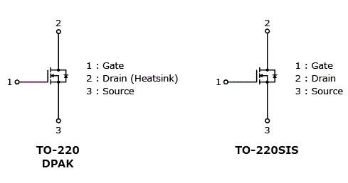
Internal Circuits
Application Circuit Examples
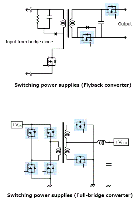
Note: The application circuits shown in this document are provided for reference purposes only.
Thorough evaluation is required, especially at the mass production design stage.
Providing these application circuit examples does not grant any license for industrial property rights.
* Information in this document, including product prices and specifications, content of services and contact information, is current on the date of the announcement but is subject to change without prior notice.
Source:http://www.semicon.toshiba.co.jp/eng/