 sales@aoelectronics.com
 +86 755 2821 9272


- Abracon
- Adam Tech
- Aerospace, Defense & Marine
- Agastat
- AIC
- AKM Semiconductor
- Alcoswitch
- Allegro
- Alps Electric
- Altera
- AMI Semiconductor
- AMP
- ams
- Analog Devices (ADI)
- Aptina Imaging
- Atmel
- Avago / Broadcom
- AVX
- Axicom
- Bccomponents
- Beyschlag
- BI Technologies
- Bourns Inc.
- Bowei Integrated Circuits
- Bridgelux
- Buchanan
- California Micro Devices
- Catalyst Semiconductor
- CGS
- Cirrus Logic
- Citizen Electronics
- CML Microcircuits
- Coiltronics
- Cooper Bussmann
- Corcom
- Core Logic
- Cree
- CSR PLC
- CTS
- Cypress Semiconductor
- Dale
- Data Image
- Deutsch
- Diodes Incorporated
- DOMINANT Opto Technologies
- E-T-A
- Eaton
- ECS
- Edison Opto
- Elcon
- EPCOS
- Epistar
- Epson
- Everlight Electronics
- Exar
- Fairchild Semiconductor
- FCI
- Freescale Semiconductor
- Fremont Micro Devices (FMD)
- Fujitsu Semiconductor
- Fulltech Electric
- General Semiconductor
- Harvatek
- Holsworthy
- Hsuan Mao Technology
- IDT
- Infineon Technologies
- Innolux
- International Rectifier (IR)
- Intersil
- IRC
- ISSI
- IXYS-IC
- Jing Cheng Electronical
- JL World
- Johanson Dielectrics
- Johanson Technology
- JRC / NJR
- JST
- KEC
- Kilovac
- Kingbright
- Kyocera Industrial Ceramics
- LEDiL
- Linear Technology / ADI
- Lite-On Technology
- Littelfuse
- Lumex
- Lumileds
- Luminary Micro
- Luminus Devices
- Macronix
- Maojwei / ZJPT
- Maxim Integrated
- MCC
- Mean Well Enterprises
- Microchip Technology
- Micron
- Microsemi
- Mini-Circuits
- Molex
- Murata Manufacturing
- Murata Power Solutions
- MWT
- National Semiconductor
- Nichicon
- Nippon Chemi-Con
- NJR / JRC
- NVE
- NXP Semiconductors
- OEG
- Omnivision
- ON Semiconductor
- Optek Technology
- Optrex
- OSRAM Opto Semiconductors
- OTAX
- Panasonic
- Peregrine(pSemi)
- Potter & Brumfield
- Power Integrations
- PowerStor
- Preci-Dip
- Prewell
- Products Unlimited
- Pulse Electronics
- PulseCore Semiconductor
- Qorvo
- Raychem
- Renesas Electronics
- RFMD
- Richtek Technology
- ROHM Semiconductor
- Rubycon
- Samsung Electro-Mechanics
- Samsung Semiconductor
- Schaffner
- Schrack
- Seiko Instruments, Inc. (SII)
- Semtech
- Sensata
- Seoul Semiconductor
- Sfernice
- Sharp Display
- Sharp Microelectronics
- Silicon Labs
- Siliconix
- Skyworks Solutions
- SoniCrest / JL World
- Spansion
- Sprague
- Stanley Electric
- STMicroelectronics
- Sunny Electronics
- Susumu (SSM)
- Taimag
- Taiyo Yuden
- TDK
- TDK-Lambda
- TE Connectivity
- Teccor
- Texas Instruments (TI)
- Thin Film
- Tianma Micro-electronics
- TOCOS
- TOKO
- Toshiba Electronic Components
- TT Electronics
- Tusonix
- TXC
- Tyntek
- Vishay
- Vishay Precision Group
- Vitramon
- Walsin Technology
- Weidmuller
- Welwyn
- Wickmann
- Winbond
- Xilinx
- Yageo
- Zetex Semiconductors
- ZJPT / Maojwei
News
Expansion of the lineup of input and output full range operational amplifiers for sensors for mobile devices that contribute to long-term operation : TC75S103F
2020-10-05 | Return Toshiba Electronic Devices & Storage Corporation has commercialized and has expanded our line-up with the launch of “TC75S103F,” a low consumption current, input and output full range CMOS operational amplifier suitable for various sensors[1] of mobile devices[2].
The new product features a typical supply current as low as 100 μA, which helps to reduce the power consumption of the device and drive the mobile device[2] for long periods of time. The new product features input and output full range (input and output Rail-to-Rail) and the minimum supply voltage is 1.8 V, enabling low voltage drive. In addition, the maximum input offset voltage is as low as 1.5 mV, which contributes to improving sensibility of sensor.
Demand for operational amplifier with low consumption and low voltage drive is increasing due to the increased number of IoT equipment and the use of a wide variety of sensors[1] in mobile devices[2]. To meet these requirements, we have developed this product onto our lineup.
Notes :
[1] Optical sensor, ultrasonic sensor, pressure sensor, vibration detection sensor, etc.
[2] Laptop PCs, digital still cameras, handheld POS terminals, pedometers, etc.
Features
Low supply current : IDD=100 μA (typ.) @VDD=1.8 V
Input and output full range (Input and output Rail-to-Rail)
Low operating voltage range : VDD-VSS=1.8 V (min)
Low input offset voltage : VIO=1.5 mV (max) @VDD=1.8 V
Applications
Various sensors[1] of mobile devices[2]
IoT equipments
Consumer equipments
Product Specifications
(Unless otherwise specified, @Ta=25 °C)
Part |
Operating |
Electrical characteristics |
|||||||
Supply |
Supply |
Input |
Source |
Sink |
Unity gain |
||||
typ. |
max |
||||||||
1.8 to 5.5 |
100 |
165 |
1.5 |
2 |
2 |
0.3 |
|||
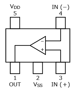
Pin Assignment (top view)
Application Circuit Example
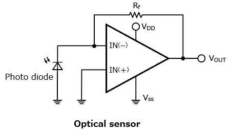
The application circuits shown in this document are provided for reference purposes only.
Thorough evaluation is required, especially at the mass production design stage.
Providing these application circuit examples does not grant any license for industrial property rights.
Information in this document, including product prices and specifications, content of services and contact information, is correct on the date of the announcement but is subject to change without prior notice.
Source:http://www.semicon.toshiba.co.jp/eng/