 sales@aoelectronics.com
 +86 755 2821 9272


Manufacturers
- Abracon
- Adam Tech
- Aerospace, Defense & Marine
- Agastat
- AIC
- AKM Semiconductor
- Alcoswitch
- Allegro
- Alps Electric
- Altera
- AMI Semiconductor
- AMP
- ams
- Analog Devices (ADI)
- Aptina Imaging
- Atmel
- Avago / Broadcom
- AVX
- Axicom
- Bccomponents
- Beyschlag
- BI Technologies
- Bourns Inc.
- Bowei Integrated Circuits
- Bridgelux
- Buchanan
- California Micro Devices
- Catalyst Semiconductor
- CGS
- Cirrus Logic
- Citizen Electronics
- CML Microcircuits
- Coiltronics
- Cooper Bussmann
- Corcom
- Core Logic
- Cree
- CSR PLC
- CTS
- Cypress Semiconductor
- Dale
- Data Image
- Deutsch
- Diodes Incorporated
- DOMINANT Opto Technologies
- E-T-A
- Eaton
- ECS
- Edison Opto
- Elcon
- EPCOS
- Epistar
- Epson
- Everlight Electronics
- Exar
- Fairchild Semiconductor
- FCI
- Freescale Semiconductor
- Fremont Micro Devices (FMD)
- Fujitsu Semiconductor
- Fulltech Electric
- General Semiconductor
- Harvatek
- Holsworthy
- Hsuan Mao Technology
- IDT
- Infineon Technologies
- Innolux
- International Rectifier (IR)
- Intersil
- IRC
- ISSI
- IXYS-IC
- Jing Cheng Electronical
- JL World
- Johanson Dielectrics
- Johanson Technology
- JRC / NJR
- JST
- KEC
- Kilovac
- Kingbright
- Kyocera Industrial Ceramics
- LEDiL
- Linear Technology / ADI
- Lite-On Technology
- Littelfuse
- Lumex
- Lumileds
- Luminary Micro
- Luminus Devices
- Macronix
- Maojwei / ZJPT
- Maxim Integrated
- MCC
- Mean Well Enterprises
- Microchip Technology
- Micron
- Microsemi
- Mini-Circuits
- Molex
- Murata Manufacturing
- Murata Power Solutions
- MWT
- National Semiconductor
- Nichicon
- Nippon Chemi-Con
- NJR / JRC
- NVE
- NXP Semiconductors
- OEG
- Omnivision
- ON Semiconductor
- Optek Technology
- Optrex
- OSRAM Opto Semiconductors
- OTAX
- Panasonic
- Peregrine(pSemi)
- Potter & Brumfield
- Power Integrations
- PowerStor
- Preci-Dip
- Prewell
- Products Unlimited
- Pulse Electronics
- PulseCore Semiconductor
- Qorvo
- Raychem
- Renesas Electronics
- RFMD
- Richtek Technology
- ROHM Semiconductor
- Rubycon
- Samsung Electro-Mechanics
- Samsung Semiconductor
- Schaffner
- Schrack
- Seiko Instruments, Inc. (SII)
- Semtech
- Sensata
- Seoul Semiconductor
- Sfernice
- Sharp Display
- Sharp Microelectronics
- Silicon Labs
- Siliconix
- Skyworks Solutions
- SoniCrest / JL World
- Spansion
- Sprague
- Stanley Electric
- STMicroelectronics
- Sunny Electronics
- Susumu (SSM)
- Taimag
- Taiyo Yuden
- TDK
- TDK-Lambda
- TE Connectivity
- Teccor
- Texas Instruments (TI)
- Thin Film
- Tianma Micro-electronics
- TOCOS
- TOKO
- Toshiba Electronic Components
- TT Electronics
- Tusonix
- TXC
- Tyntek
- Vishay
- Vishay Precision Group
- Vitramon
- Walsin Technology
- Weidmuller
- Welwyn
- Wickmann
- Winbond
- Xilinx
- Yageo
- Zetex Semiconductors
- ZJPT / Maojwei
News
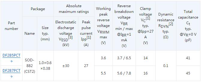
Bidirectional TVS diode with a higher peak pulse current rating that contributes to improving reliability of the IC’s power supply lines : DF2B5PCT, DF2B7PCT
2020-05-22 | Return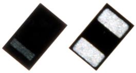 Toshiba Electronic Devices & Storage Corporation has launched bidirectional TVS diodes (ESD protection diodes), “DF2B5PCT” and “DF2B7PCT”, which have increased the peak pulse current rating of standard capacitance types suitable for power supply lines of ICs.
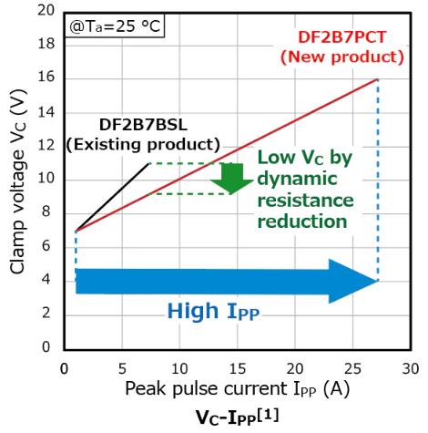
New products feature a peak pulse current rating[1] of 27 A and a typical dynamic resistance[2] of 0.1 Ω. Compared with DF2B7BSL, which is a bidirectional TVS diode with a high peak pulse current rating[1], the ESD absorbing performance improves about three times the peak pulse current[1], and about 50 % reduction in the typical dynamic resistance[2] and a low clamp voltage[1]. Therefore, it contributes to the improvement of reliability.
The new product lineup includes DF2B7PCT for the standard 5 V power supply line and DF2B5PCT for the 3.3 V power supply line. By selecting a TVS diode suitable for the power supply voltage, excessive applied voltage, which is generated at power supplies in transient state, to the ICs and another parts to be protected in following stages can be suppressed and damage can be prevented.
The package uses a small SOD-882 (Toshiba’s package name : CST2). Since the mounting area of the board can be reduced, it can be used for various applications besides mobile devices.
Due to lowering ESD capacity derived from miniaturization process of ICs, reliability requirements for mobile devices such as smartphones and tablets are increasing. In addition, the protective device itself requires a high peak pulse current because the device must be protected from transient overvoltages caused by ESD, induced lightning, and poor power supply quality. To meet these demands, we have developed a lineup of new products with high peak pulse current ratings and low dynamic resistance.
Notes:
[1] @IEC61000-4-5 (tp=8/20 μs)
[2] TLP parameters : Z0=50 Ω, tp=100 ns, tr=300 ps, averaging window : t1=30 ns to t2=60 ns, extraction of dynamic resistance using least squares fit of TLP characteristics between IPP1=8 A and IPP2=30 A.
Features
High peak pulse current rating[1] : IPP=27 A
Low dynamic resistance[2] : RDYN=0.1 Ω (typ.)
Low clamp voltage[1] :
- VC=14 V (typ.) @IPP=27 A (DF2B5PCT)
- VC=16 V (typ.) @IPP=27 A (DF2B7PCT)
High electrostatic discharge voltage rating[3] : VESD=±30 kV
Working peak reverse voltage :
- VRWM=3.6 V (max) (DF2B5PCT)
- VRWM=5.5 V (max) (DF2B7PCT)
Notes:
[3] @IEC61000-4-2 (Contact)
Applications
Smart phones
Tablets
Game consoles, etc.
Product Specifications
(@Ta=25 °C)
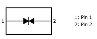
Internal Circuit
Application Circuit Example
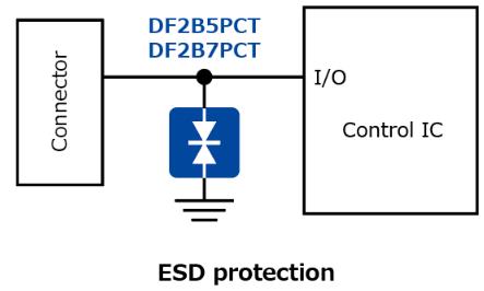
The application circuits shown in this document are provided for reference purposes only. Thorough evaluation is required, especially at the mass-production design stage. Providing these application circuit examples does not grant any license for industrial property rights.
Characteristic figure (Reference)
Information in this document, including product prices and specifications, content of services and contact information, is correct on the date of the announcement but is subject to change without prior notice.
Source:http://www.semicon.toshiba.co.jp/eng/